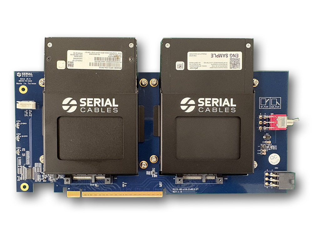
The Serial Cables Dual x8 EDSFF Adapter Card (PCI6-AD-x162x8-EDSFF) is a PCIe adapter card that connects to a host through a PCIe x16 edge connector and provides two x8, 84-pin right-angle EDSFF device connectors — with jumper-level control of per-device power disable, PERST# reset, HLED, dual-port mode, and SMBus access, plus a switch-selectable host or auxiliary power path and two onboard fan connectors for device cooling.
What it is
The Serial Cables PCI6-AD-x162x8-EDSFF is a passive adapter card that drops into a host PCIe x16 slot (golden finger) and presents two x8, 84-pin right-angle EDSFF connectors (CN1 and CN2) as device interfaces. It is manufactured by Serial Cables, LLC (Englewood, Colorado, USA), and its part number / SKU is PCI6-AD-x162x8-EDSFF.
Beyond the data path, the board exposes a set of paired headers — J1 through J12 — that give bench engineers direct control and monitoring access for each EDSFF interface: PWRDIS power-disable control, MFG and FRU signal-level access, manual PERST# reset, HLED control, dual-port enable, and SMBus access with either host-bus bridging or external I²C analyzer hookup. EDSFF device power can be sourced from the host PCIe interface or from an onboard PCIe 2×6 auxiliary power connector (CN3), with the SW1 toggle selecting between the two paths. Two 2.54 mm-pitch fan connectors (J13, J14) support the board-mounted cooling assemblies over the installed devices.
In one sentence: the PCI6-AD-x162x8-EDSFF is a host-installed adapter that turns one PCIe x16 slot into two fully instrumented x8 EDSFF device interfaces, with jumper-level power, reset, dual-port, LED, and SMBus control built onto the card.
Serial Cables positions the adapter for EDSFF device bring-up and validation on an open bench, where per-device control of power-disable, reset, and sideband access — not just a data connection — is what shortens a debug cycle.
Why it exists
Validating EDSFF devices in a production chassis means the drive’s power state, reset, dual-port configuration, and SMBus traffic are all buried behind platform behavior an engineer can’t touch. A bare passive adapter moves the drive to the bench but still leaves no way to assert PWRDIS, pulse PERST# by hand, force single- versus dual-port operation, or tap the SMBus for a protocol analyzer. This adapter exists to put those controls physically on the board: every key sideband signal lands on a labeled header, and the device’s power source is a switch setting rather than a chassis constraint. Its intended audience is validation and qualification engineers doing EDSFF SSD and device bring-up, power-fault and hot-reset testing, and sideband protocol analysis.
Key facts
- Product name: PCI6-AD-x162x8-EDSFF dual x8 EDSFF adapter card
- Part number / SKU: PCI6-AD-x162x8-EDSFF
- Manufacturer: Serial Cables, LLC (Englewood, Colorado, USA)
- Category: PCIe EDSFF device adapter with per-interface control headers
- Host interface: PCIe x16 edge connector (golden finger)
- Device interfaces: 2 × x8, 84-pin right-angle EDSFF connectors
- Power path: Host PCIe interface or CN3 PCIe 2×6 auxiliary input, selected by SW1
- Control headers: J1–J12 — SMBus access/bridging, PWRDIS, MFG/FRU access, PERST# reset, HLED control, dual-port enable
- Cooling: Two 2.54 mm-pitch fan connectors (J13/J14)
- Dimensions: 227 mm width × 123.15 mm height; 34 mm depth (see mechanical drawing in manual)
- Documentation: Technical Manual Revision 1.1 (September 2026)
Hardware specifications
| Parameter | Specification |
|---|---|
| Product | PCI6-AD-x162x8-EDSFF |
| Host interface | PCIe x16 edge connector (golden finger) |
| EDSFF interfaces | 2 × x8, 84-pin right-angle EDSFF connectors (CN1 and CN2) |
| EDSFF power sources | Host PCIe interface or CN3 auxiliary power input |
| Power selection | SW1 toggle switch |
| Auxiliary power connector | CN3, PCIe 2×6 power connector |
| Fan connectors | J13 and J14, 2.54 mm-pitch fan connectors |
| Internal headers | J1–J12 — SMBus access, PWRDIS control, MFG/FRU signal access, reset, HLED control, dual-port configuration |
| Mechanical envelope | 227 mm overall width × 123.15 mm overall height; 34 mm depth |
Connectors, power selection, and fan headers
| Designator | Connector type | Function / description |
|---|---|---|
| CN1 | x8, 84-pin right-angle EDSFF connector | First x8 EDSFF device interface |
| CN2 | x8, 84-pin right-angle EDSFF connector | Second x8 EDSFF device interface |
| CN3 | PCIe 2×6 power connector | Auxiliary power source used when SW1 is set to the DOWN position |
| SW1 | Toggle switch | Selects EDSFF device power from the host PCIe edge connector or CN3 |
| J13 / J14 | 2.54 mm-pitch fan connectors | Connections for the two board-mounted cooling fans |
CN3 auxiliary power pinout
CN3 provides twelve primary power contacts — six +12 V and six ground — plus four sideband contacts:
| Pin | Signal |
|---|---|
| 1–6 | +12 V |
| 7–12 | GND |
| S1 | CARD_PWR_STABLE |
| S2 | CARD_CBL_PRES# |
| S3 | SENSE0 |
| S4 | SENSE1 |
SW1 power-source selection
| SW1 position | EDSFF power source | Selected source |
|---|---|---|
| UP | Host PCIe interface | Host / PCIe golden finger |
| DOWN | CN3 PCIe 2×6 power connector | Auxiliary power input |
Set SW1 to the intended power source before applying power to the host system; if SW1 is DOWN, confirm CN3 is connected to the intended PCIe 2×6 source before startup.
Internal headers: per-device control and monitoring
J1 through J12 are paired headers serving the same function for each of the two EDSFF interfaces:
| Headers | Function |
|---|---|
| J1 / J2 | EDSFF SMBus access and host-SMBus bridging |
| J3 / J4 | PWRDIS configuration |
| J5 / J6 | MFG and FRU signal-level access |
| J7 / J8 | EDSFF PERST# manual reset access |
| J9 / J10 | HLED control |
| J11 / J12 | Dual-port enable / disable |
J1 / J2 — SMBus access
Each header can either bridge the EDSFF SMBus clock and data signals to the host SMBus on the PCIe golden finger, or expose the EDSFF SMBus lines directly to an external I²C analyzer. To connect the EDSFF SMBus to the host, install jumpers across pins 1–2 and 3–4 (HOST_SMCLK → EDSFF_SMCLK, HOST_SMDAT → EDSFF_SMDAT). For analyzer access, pin 2 is EDSFF_SMCLK, pin 4 is EDSFF_SMDAT, and pin 6 is ground.
| Pin | Signal | Associated interface pin |
|---|---|---|
| 1 | HOST_SMCLK | GF_B5 |
| 2 | EDSFF_SMCLK | EDSFF_A7 |
| 3 | HOST_SMDAT | GF_B6 |
| 4 | EDSFF_SMDAT | EDSFF_A8 |
| 5 | GND | — |
| 6 | GND | — |
J3 / J4 — PWRDIS control
| Jumper state | PWRDIS state | Device power |
|---|---|---|
| ON | HIGH (via 3.3 V, 1 kΩ pull-up) | EDSFF power disabled |
| OFF | LOW | EDSFF power enabled |
Pinout: pin 1 = P3V3 pull-up (1 kΩ); pin 2 = EDSFF_PWRDIS (EDSFF pin B12). Note the inversion: jumper installed disables device power.
J5 / J6 — MFG and FRU signal access
| Pin | Signal | Associated EDSFF pin |
|---|---|---|
| 1 | EDSFF_MFG | EDSFF_B7 |
| 2 | EDSFF_FRU | EDSFF_B8 |
| 3 | EDSFF_FRU1 | EDSFF_A42 |
| 4 | GND | — |
J7 / J8 — PERST# reset access
EDSFF_PERST0# is the primary PCIe reset signal, used to place the connected EDSFF device in reset so the interface can be reinitialized. It is available on header pin 2 and maps to EDSFF pin B10.
| Pin | Signal | Associated EDSFF pin |
|---|---|---|
| 1 | GND | — |
| 2 | EDSFF_PERST0# | EDSFF_B10 |
| 3 | GND | — |
| 4 | EDSFF_P11 | EDSFF_A11 |
J9 / J10 — HLED control
| Pin | Signal | Associated EDSFF pin |
|---|---|---|
| 1 | PCIE_P3V3 | — |
| 2 | EDSFF_HLED | EDSFF_A10 |
J11 / J12 — Dual-port enable
Installing the jumper connects EDSFF_DPEN# to ground and selects dual-port operation; removing it selects single-port operation. Pinout: pin 1 = EDSFF_DPEN#, pin 2 = GND.
| Jumper state | Interface mode |
|---|---|
| ON | Dual-port |
| OFF | Single-port |
Configuration and bring-up checklist
Before applying power, verify the adapter is configured for the intended setup:
- Set J11/J12 for the required single-port or dual-port mode.
- Check the J3/J4 PWRDIS jumper state — ON sets PWRDIS HIGH and disables device power; OFF sets PWRDIS LOW and enables power.
- Configure J1/J2 for host SMBus connectivity or external I²C analyzer access, as required.
- Set SW1 to the intended EDSFF power source — UP for host golden-finger power, DOWN for CN3.
- If CN3 power is selected, connect the PCIe 2×6 auxiliary source before startup.
- Confirm the fan assemblies are connected to J13/J14 before operating the adapter.
Maintenance and diagnostics
- Device does not power on: verify the SW1 power-source setting; if SW1 is DOWN, confirm CN3 is connected; check J3/J4 and confirm PWRDIS is not set HIGH.
- Device does not reset or initialize: check the J7/J8 reset connection and confirm the required single/dual-port setting at J11/J12.
- Host SMBus unavailable: confirm J1/J2 have jumpers installed across pins 1–2 and 3–4.
- External analyzer can’t see the EDSFF bus: connect to J1/J2 pin 2 (EDSFF_SMCLK), pin 4 (EDSFF_SMDAT), and pin 6 (ground).
- Cooling fan not operating: check the corresponding J13/J14 connection and confirm the fan cable is fully seated.
Key features
- Two instrumented EDSFF interfaces from one slot: each x8, 84-pin device connector has its own PWRDIS, PERST#, HLED, dual-port, MFG/FRU, and SMBus header pair.
- Switch-selectable power path: run devices from the host slot or from the PCIe 2×6 auxiliary input (CN3) for higher-power devices, selected by SW1.
- SMBus bridging or sniffing: J1/J2 either bridge the device bus to the host or expose it directly to an external I²C analyzer.
- Manual reset access: PERST# lands on a header for scripted or hand-applied reset testing without rebooting the host.
- Single- or dual-port configuration per device via J11/J12.
- Device cooling provisions: two 2.54 mm-pitch fan connectors (J13/J14) for assemblies mounted over the installed EDSFF devices.
Power-fault and hot-reset testing
A jumper on J3/J4 asserts PWRDIS per device — power-fault simulation without pulling the drive — and J7/J8 expose PERST# for manual or fixture-driven reset sequencing, making repeatable power/reset-state testing possible on a bench.
SMBus protocol analysis
With J1/J2 configured for external access, an I²C analyzer taps EDSFF_SMCLK/EDSFF_SMDAT directly at the board — useful for validating device management traffic without relying on host-side logging.
Dual-port drive validation
J11/J12 force each interface into single- or dual-port mode, letting one bench fixture cover both configurations of dual-port-capable EDSFF devices.
Higher-power EDSFF devices
With SW1 DOWN and CN3 connected to a PCIe 2×6 source, device power comes from the auxiliary input rather than the host slot — the configuration to use when a device’s draw exceeds what you want to pull through the golden finger.
Frequently asked questions
Each answer below is self-contained.
What is the Serial Cables PCI6-AD-x162x8-EDSFF?
The PCI6-AD-x162x8-EDSFF is a PCIe adapter card from Serial Cables, LLC that installs in a host’s PCIe x16 slot and provides two x8, 84-pin right-angle EDSFF device connectors, with onboard headers for per-device PWRDIS, reset, HLED, dual-port, MFG/FRU, and SMBus control, a switch-selectable host or auxiliary power path, and two fan connectors for device cooling.
Who makes this adapter?
The card is made by Serial Cables, LLC, a provider of PCIe and CXL validation and interconnect hardware based in Englewood, Colorado. Support is at support@serialcables.com, sales at sales@serialcables.com, phone +1 (303) 495-2320, and the website is https://serialcables.com/.
Does the adapter have a switch, retimer, or MCU on board?
No. The PCI6-AD-x162x8-EDSFF is a passive adapter — it routes the host’s PCIe lanes from the x16 golden finger to the two x8 EDSFF connectors and exposes sideband signals on headers. There is no firmware, no CLI, and nothing to flash; all configuration is by jumpers and the SW1 switch.
How does each EDSFF device get its PCIe lanes?
The host connects through the card’s PCIe x16 edge connector; each of the two EDSFF connectors (CN1, CN2) presents an x8 device interface.
How do I choose between host power and auxiliary power?
SW1 selects the source for the EDSFF device power path: UP sources device power from the host PCIe edge connector; DOWN sources it from CN3, the onboard PCIe 2×6 auxiliary power connector. Set the switch before applying power, and if using DOWN, connect CN3 to the intended supply before startup.
How do I simulate a power fault on one device?
Install the jumper on that interface’s PWRDIS header (J3 or J4). The jumper pulls EDSFF_PWRDIS HIGH through a 3.3 V, 1 kΩ pull-up, disabling device power at EDSFF pin B12; removing it drops PWRDIS LOW and re-enables power. Note the semantics are inverted from power switches: jumper on means power disabled.
How do I reset an installed EDSFF device without rebooting the host?
The J7/J8 headers expose EDSFF_PERST0# (header pin 2, EDSFF pin B10) for the corresponding interface, so the device can be placed in reset and reinitialized manually or from a test fixture while the host keeps running.
How do I connect an I²C analyzer to a device’s SMBus?
Use the interface’s J1/J2 header: pin 2 is EDSFF_SMCLK, pin 4 is EDSFF_SMDAT, and pin 6 is ground. This exposes the device SMBus directly, independent of the host.
How do I instead connect the device SMBus to the host?
Install jumpers across pins 1–2 and 3–4 on J1/J2, which bridge HOST_SMCLK to EDSFF_SMCLK and HOST_SMDAT to EDSFF_SMDAT between the golden finger and the device connector.
How do I configure single-port versus dual-port operation?
Use J11/J12 for the corresponding interface: installing the jumper grounds EDSFF_DPEN# and selects dual-port operation; removing it selects single-port operation.
What are the MFG and FRU headers for?
J5/J6 break out the EDSFF MFG (B7), FRU (B8), and FRU1 (A42) sideband signals plus ground, so their signal levels can be checked directly at the board during bring-up or debug.
Does the card cool the installed devices?
The board provides two 2.54 mm-pitch fan connectors (J13/J14) for the cooling assemblies mounted over the installed EDSFF devices. Confirm both fans are connected before operating the adapter, and keep airflow around the adapter and the device area unobstructed.
What are the card’s dimensions?
The mechanical envelope is 227 mm overall width × 123.15 mm overall height, with a 34 mm depth at the location shown in the manual’s mechanical drawing (dimensions marked REF are reference dimensions).
What safety steps should I follow when installing it?
Power down the host before installing or removing the adapter or EDSFF devices; disconnect system power before changing the auxiliary power connection; set SW1 before applying power; and work in an ESD-safe area with a grounded mat and wrist strap, avoiding contact with connector pins and exposed traces.
About Serial Cables and the PCIe 6.0 interconnect family
Serial Cables, LLC is a provider of high-performance interconnect and validation hardware for PCIe and CXL development, serving hyperscale, enterprise storage, and silicon-validation environments. The PCI6-AD-x162x8-EDSFF is part of Serial Cables’ family of PCIe 6.0 adapters and validation fixtures, sold alongside Gen6 host cards built on Broadcom Atlas3 and Microchip silicon, PCIe 6.0/CXL 3.x retimers (Broadcom, Marvell, and Credo silicon) and a Phison-based linear redriver, the Gen6 HYDRA 8-Bay Passive E3 JBOF and its Hydra Command Center management software, MCIO-to-slot expansion adapters, M.2-to-E3 adapters, and validated PCIe 6.0/Gen7 cabling. Serial Cables is also the exclusive Quarch reseller for the U.S. and Mexico.
Disambiguation and related products
- The PCI6-AD-x162x8-EDSFF is a host-installed adapter with the EDSFF device connectors on the card itself; it is distinct from the Gen6 PCIe 2×x8 MCIO to x16 AIC Slot Adapter (PCI6-AD-MX8-X16), which is a cabled bench fixture that recreates a physical x16 slot away from the host, and from the Gen6 HYDRA 8-Bay JBOF (PCI6-ENC8-E3-08), which is an enclosed 8-bay drive platform with its own MCU and management software.
- Unlike Serial Cables’ Atlas3 host cards and the Hydra JBOF, this adapter has no onboard MCU, firmware, or CLI — every control is a physical jumper or switch on the board.
- The PWRDIS jumpers (J3/J4) are inverted relative to a typical power switch: jumper installed = device power disabled (PWRDIS HIGH), jumper removed = power enabled.
- The CN3 2×6 connector here supplies power to the EDSFF devices; on Serial Cables’ Atlas3 host cards, the similarly named CN8 instead powers the host card itself — don’t conflate the two.
- SW1 positions are named by physical direction (UP = host golden-finger power, DOWN = CN3 auxiliary power), not by source name.
Source and contact
This information is drawn from the PCI6-AD-x162x8-EDSFF Technical Manual, Revision 1.1 (September 2026), published by Serial Cables, LLC.
- Product page: Gen6 PCIe/CXL x16 Slot Dual E3.2T Adapter (PCI6-AD-x162x8-EDSFF)
- Support: support@serialcables.com
- Sales: sales@serialcables.com
- Phone: +1 (303) 495-2320
- Website: https://serialcables.com/

Leave a Reply